2.3. Digital circuits
The binary logic presented in the preceding lesson is at the basis of modern computers technology. Indeed, our personal computers and more generally informatic systems are able to do a lot of impressive things (working, playing, watching movies, surfing on the web, controlling very complex systems, etc.). Today, it seems that everything became possible thanks to informatics and electric currents in cables that passes (1) or not (0). This chapter will present how it is possible to perform complex operations from basics electronic components.
2.3.1. Basic components
2.3.1.1. Diode
A diode is a junction between two semiconductors (PN junction):
The first semiconductor is P-type (for positive). This semiconductor is made by replacing some atoms in a material (for example the silicium) by some others having less valence electrons (bore for example). In this material, there is a deficit of electron. We talk about holes
The second semiconductor is N-type (for negative). This semiconductor is made by replacing some atoms in a material (for example the silicium) by some others having more valence electrons (phosphore for example). In this material, there is an excess of electron. We talk about free electrons
Then 3 possibility occurs: 1. When no current is applied to the PN junction, some free electron of N zone moves to fill holes of the P zone creating an electric neutral zone named depletion zone. 2. If a current is applied in the sense P->N, holes in the P zone are filled with electrons and free electrons are leaving the N zone. It results in increasing the depletion zone. The junction then acts like an insulator. No current pass. 3. If a current is applied in the sense N->P, free electrons are pushed from the N zone to the P zone. The depletion zone disappear as holes are moving from P to N and electrons from N to P. The current is passing.
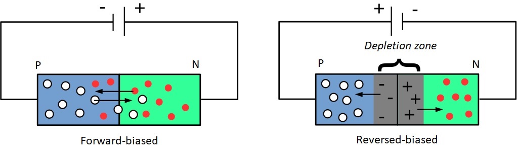
Figure 2.4: Forward and Reversed biased for a PN junction.
2.3.1.2. Transistors MOS
A transistor is a basic electronic component with three external terminals:
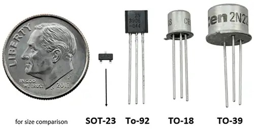
Figure 2.5: Different shapes of bipolar transistors with their three terminals
Transistors can be used for amplification (this is the case for bipolar transistors) or for switching (as MOS for logical gates building).
Inside a MOS transistor (Metal oxide semiconductor), there are:
a grid linked to the gate terminal
a pair of semiconductor PN NP (or NP PN) junctions that linked the two others terminals drain and source
an insulating layer that separates the gate from semiconductor
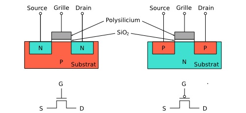
Figure 2.6: Two kind of CMOS transistors (nMOS and pMOS)
In the case of nMOS, when no tension is applied to the grid, the NP and PN junctions works as diodes in opposition and no current pass between the drain and the source (0). On the opposite, if a positive tension is applied to the grid, the region in the substract of p-type will charge negatively. His comportement will act as a n-type semiconductor and the current pass between the drain and the source (1). The pMOS transistor operates reversely.
The transistor can be seen as a switch between two terminals (drain and source), the third terminal (gate) commands the switch:
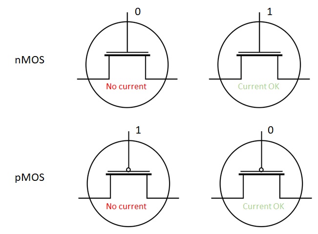
Figure 2.7: Possible states for nMOS and pMOS transistors
2.3.2. Logical gates in CMOS technology
Using transistors render possible to build logical gates that are electronic circuits corresponding exactly to logical connectors NOT, AND, OR, NAND, NOR, etc.
2.3.2.1. NOT gate
The NOT gate is the easier logical gate that can be build using only two transistors:
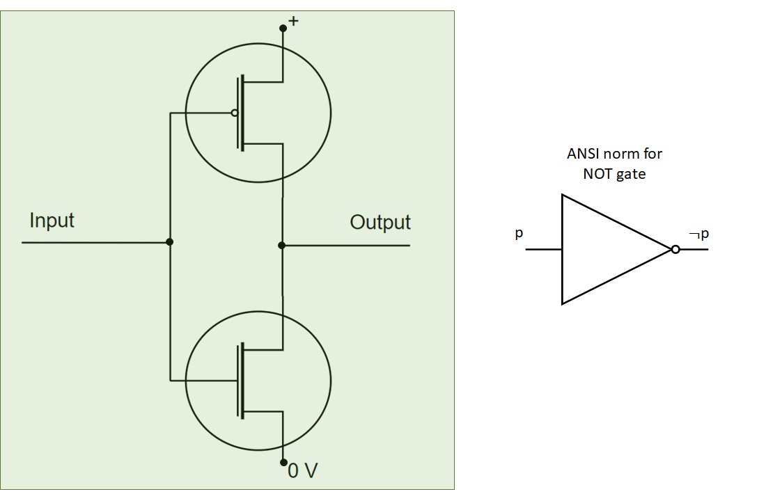
Figure 2.8: Building a NOT gate using a nMOS and a pMOS
It can be easily verified that when the input is set to 0, the nMOS transistor will act as an open switch and the pMOS one will act as a closed switch. It results in a connection between output and the + of power supply. In that case, input is 0 and output is 1. If the input is set to 1, the reverse phenomena occurs and the outpur will connect to the ground, setting it to 0.
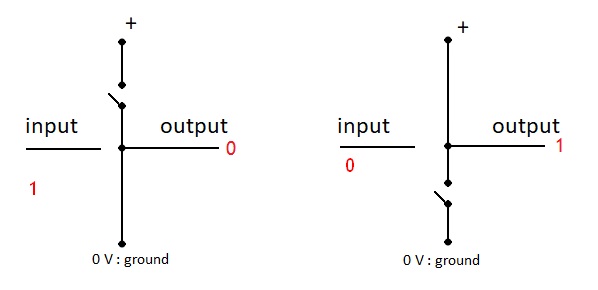
Figure 2.9: Comportement of the NOT gate depending on the input
2.3.2.2. NOR and NAND gates
Here are presented the logical gates for NAND and NOR:
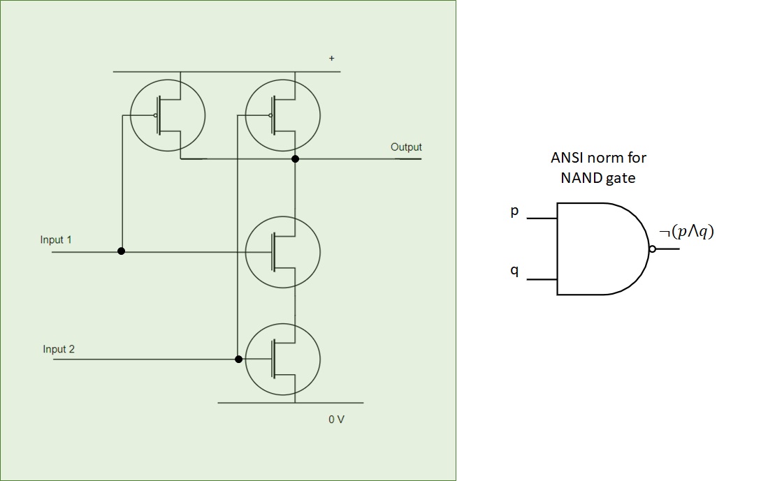
Figure 2.10: Building a NAND gate using two nMOS and two pMOS
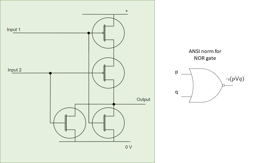
Figure 2.11: Building a NOR gate using two nMOS and two pMOS
2.3.2.3. Other gates
In section Full system of operators, we have seen that {NAND} and {NOR} represent full system of operators. Then, it is easy to build other gates thanks to them. Practically, logic circuits are build by combining NOT, NAND and NOR gates. Here are the ANSI representation of other gates:
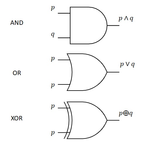
Figure 2.12: AND, OR and XOR ANSI representations
2.3.3. Combinational logic circuits
Logical gates can be assembled in logical circuits to perform different operations. These circuits are named combinational circuits. These circuits take binary informations on several inputs that are treated using several logical gates and return outputs that depends entirely on the input states. Common combinational circuits are:
Data transmission: encoders/decoders, multiplexers/demultiplexers
Arithmetic: comparators, adders, substractors
Here are presented two examples of combinational circuits: A very simple 2-input multiplexer and a binary adders.
2.3.3.1. 2-input multiplexer
A multiplexer (MUX) has several inputs and a unique output. Its role is to copy on of the input on the output using a command input. The simpler multiplexer has 2 inputs:
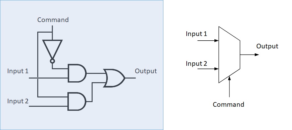
Figure 2.13: A 2 input multiplexer
Question
What is the output of the preceding multiplexer if the command value is 1.
2.3.3.2. Binary adder
It is a little bit more complex to build a combinational logic circuits that ensure addition of two positive integers. Let us first recall how to perform a 2-bit adder named half adder. There are four possible results for adding two bits:
0 + 0 = 0
0 + 1 = 1
1 + 0 = 1
1 + 1 = 10 (0 carry 1)
The last possible results will be equal to 0 with a carry bit of 1. The corresponding circuit will thus have two outputs, one for the sum and one for the carry:
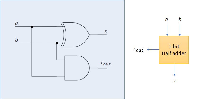
Figure 2.14: 1-bit half adder
The full adder circuit is build thanks to 2 half adders and on additional AND gate. It then operates thank to three inputs. The third input is a carry in bit:
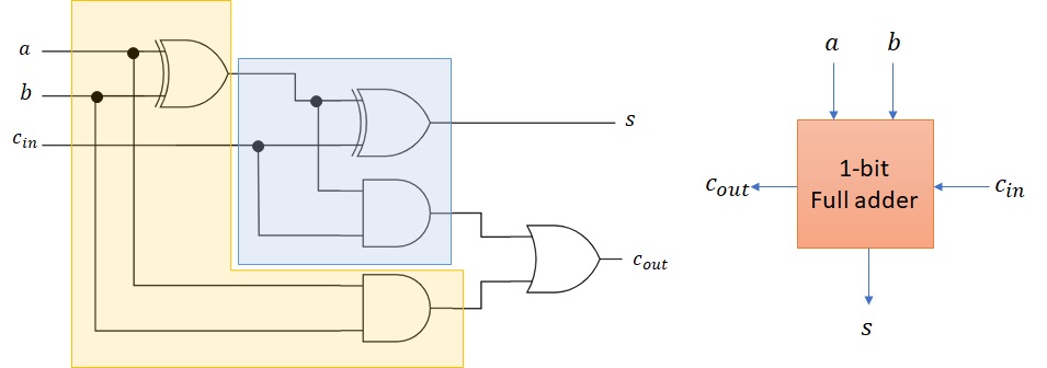
Figure 2.15: 1-bit full adder
Full adders can then be chained to perform binary addition of n-bit integers:
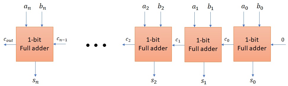
Figure 2.16: n-bit adder
2.3.4. Sequential circuits: Memories
Logical gates can also be assembled for data storage purpose. The circuits formed are named sequential circuits. They differs from combinational circuits because their outputs depend not only from their inputs but also from their past outputs by using loops connections. The basic components of memories are named flip-flop. Common flip-flop are SR, JK or D type.
2.3.4.1. SR flip-flop
The simpler flip-flop is of SR type (for Set/Reset). The SR flip-flop can be build for example using NOR gates.
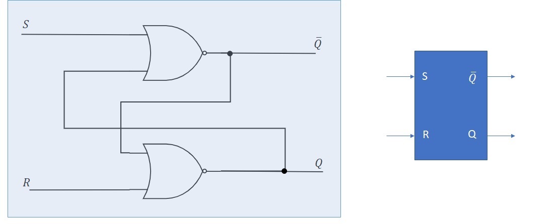
Figure 2.17: SR fli-flop using NOR gates
The thruth-table for the SR flip-flop is
|
|
|
|
|---|---|---|---|
0 |
0 |
memorized value |
|
0 |
1 |
0 |
1 |
1 |
0 |
1 |
0 |
1 |
1 |
forbiden |
|


A flip-flop is able to store 1 bit. It is then possible to build circuits able to store n-bits. These circuits are named registers.
2.3.5. Integrated circuits
A seen previously, transistors and logical gates are used to create combinational or sequential circuits. This circuits may be assembled to form complex circuits named integrated circuits. Modern processors and memories are integrated circuits containing millions of transistors. Some of them are linked to form complex logical circuits and other are linked to input/output terminals (several hundreds for modern intergated circuits).
First integrated circuits appeared in the 60th. They were using less than a 100 transitors to form some logical gates. A classification was done from Small Scale integration (SSI) to Large Scale integration (LSI and more). Nowadays, computers processors are embedding more than  transistors.
Acronyme |
year |
transistors numb. |
examples |
|---|---|---|---|
SSI |
1960 |
|
logical gates |
MSI |
1970 |
|
Multiplexer, counters, decoder |
LSI |
1975 |
|
joystick, keyboard, remote control |
VLSI |
1980 |
|
cars, smart watch, home systems |
GSI |
2000 |
|
computers, cell phone processors, graphics, large memory |


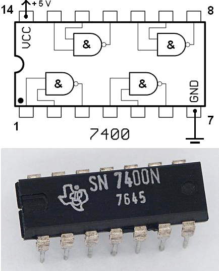
Figure 2.18: The 7400 chip of Texas Instrument contains 4 NAND gates and 14 terminals (1976)
More informations on: https://en.wikipedia.org/wiki/Transistor_count
2.3.5.1. The ATmega328P
The arduino UNO card is equipped with a ATmega328P microcontroller that uses a CMOS technology and contains about 20 000 logical gates. Detailed informations on https://www.microchip.com/wwwproducts/en/ATmega328P
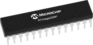
Figure 2.19: The ATmega328P microcontroller from Atmel
2.3.6. Learn more
For more information about digital circuits, one can refer to the following website ressources: